Events
About us
News
Archive
FAQs
英語
日本語
Contact
News
All
BID 2024
Brabant
Connecting ecosystems
Partnerships
29.08.2025
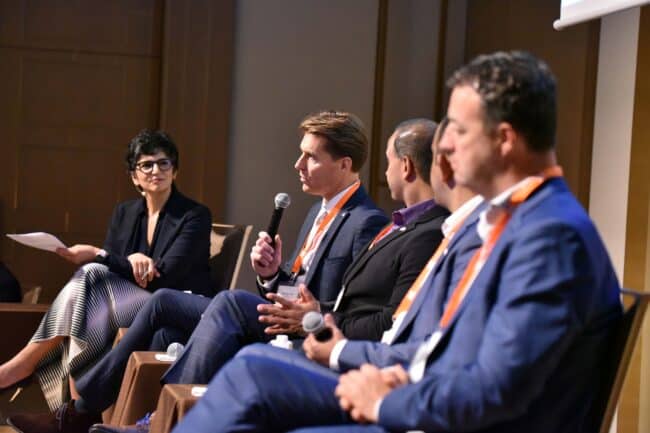
A lookback at Brabant Innovation Day 2024
BID 2024
29.08.2025
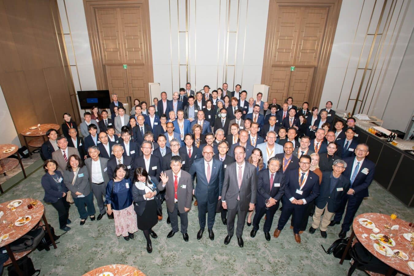
They said it: heard at Brabant Innovation Day 2024
BID 2024
25.08.2025
How PhotonDelta is powering Europe’s photonics future
Connecting ecosystems
Partnerships
22.08.2025
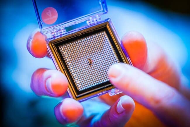
Holst Centre: Leading the way in sustainable and flexible electronics
Connecting ecosystems
Partnerships
18.08.2025
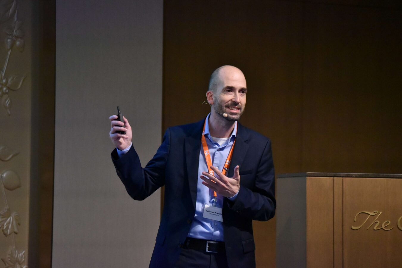
Onera Health brings hospital-grade sleep testing home to sleepless Japan
Connecting ecosystems
12.08.2025
Winning, together: how Brabant’s ecosystem accelerates innovation
Connecting ecosystems
12.08.2025
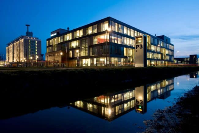
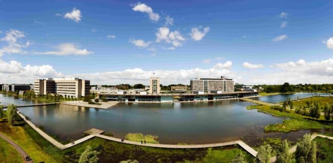
Brabant: the rise of the Netherlands’ Silicon Valley
Brabant
Register for
event
Event
(Required)
Please select event
Email
(Required)
Company
(Required)
(Required)
First name
Last name
Country
Untitled
(Required)
I agree with the privacy policy and the processing of my personal data as described in the
privacy statement
.